
How to Choose the Right Silicon Inductor?
Choosing the right Silicon Inductor requires more than comparing inductance values on a supplier page. Designers must connect the component’s electrical behavior with the real circuit, board space, operating temperature, and production goals. A compact part may look ideal, yet its quality factor can fall at the target frequency. That difference can weaken filtering, matching, or signal integrity.
Practical evaluation should begin with the required inductance, frequency range, current level, and acceptable loss. Check impedance curves, self-resonant frequency, tolerance, and temperature stability. Package dimensions also matter. A 1.0 mm component can simplify placement, but it may demand tighter assembly control. Review the manufacturer’s datasheet, qualification reports, and recommended layout details. Independent laboratory measurements are valuable when specifications appear incomplete or unusually optimistic.
Bench testing often reveals details that calculations miss. Measure insertion loss with the intended substrate, connectors, and nearby components. Inspect performance after thermal cycling, not only at room temperature. No selection method is perfect. Parasitic coupling, fixture errors, and layout changes can distort results. I have seen a promising inductor fail because the evaluation board differed from the production stack-up. That mistake was avoidable, but not obvious at first. A reliable choice therefore balances simulation, verified measurements, supplier credibility, and realistic manufacturing conditions. This guide explains those decisions clearly, helping engineers compare Silicon Inductor options without treating one impressive specification as the whole answer.
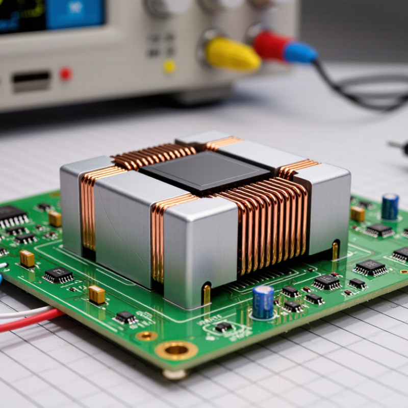
Understanding Silicon Inductors and Their Core Functions
Choosing the right silicon inductor starts with understanding what it does. A silicon inductor is an integrated passive component formed within a semiconductor process. It stores energy in a magnetic field and resists rapid changes in current. In radio-frequency circuits, it can match impedance, tune oscillators, filter unwanted signals, or connect an antenna network. Its small footprint matters. So does its electrical behavior.
The core specifications deserve careful reading. Inductance sets the expected reactance at a target frequency. Quality factor indicates how much energy is lost, while self-resonant frequency marks where parasitic capacitance changes performance. Current handling and resistance also affect heating and signal loss. Measure under realistic temperature and frequency conditions. A room-temperature result may mislead. Layout is equally important; nearby metal, ground planes, and routing can shift the measured value.
For selection, match inductance, tolerance, Q value, and operating frequency to the circuit function. Check model accuracy before trusting simulation results. In practice, a network analyzer and controlled test fixture reveal details that a datasheet may hide. I would also compare two footprints, because a smaller part is not automatically better. That assumption fails surprisingly often. Leave design margin for process variation and temperature drift. Some choices remain imperfect when efficiency, size, and bandwidth conflict. Recheck the circuit after assembly, not only on paper.
| Selection Dimension | What It Means | Representative Silicon-Inductor Data | Selection Guidance |
|---|---|---|---|
| Primary Function | Defines how the inductor is used in the circuit. | RF matching, filtering, resonance, impedance transformation, and supply-noise isolation | Choose the component according to the circuit objective rather than inductance alone. A matching network may prioritize Q, while a power or bias network may prioritize current handling. |
| Inductance Value | The nominal opposition to changes in current, expressed in nanohenries for most integrated RF applications. | Approximately 0.5–100 nH; many RF designs use about 1–30 nH | Select the value required by the target frequency and matching topology. Confirm the effective inductance at the actual operating frequency. |
| Operating Frequency | The frequency range over which the component maintains acceptable electrical performance. | Commonly hundreds of MHz to several GHz | Use measured or modeled S-parameters at the intended frequency. Parasitic capacitance and substrate loss become increasingly important as frequency rises. |
| Quality Factor (Q) | The ratio of reactive energy to resistive energy loss; higher Q generally indicates lower loss. | Typically about 5–30 at RF, depending on frequency, geometry, and process | Choose a higher-Q device for narrowband matching, resonators, and low-loss filters. Moderate Q may be adequate for broadband matching or damping applications. |
| Self-Resonant Frequency (SRF) | The frequency at which inductive and parasitic capacitive effects resonate. | Often approximately 1–20 GHz for integrated RF structures | Keep the operating frequency comfortably below the SRF. Near or above SRF, the component may behave capacitively instead of inductively. |
| DC Resistance (DCR) | The resistance of the conductive path measured at or near direct current. | Approximately 0.1–10 Ω, depending on inductance, metal width, and layout | Lower DCR reduces conduction loss and voltage drop. Check the complete signal or bias path because substrate and metal losses also affect RF performance. |
| Current Handling | The current level that can be carried without excessive heating, electromigration risk, or unacceptable performance shift. | Often from several mA to a few hundred mA for integrated structures | Verify continuous and peak current separately. Integrated silicon inductors are generally intended for RF and signal applications, not high-current power conversion. |
| Tolerance | The allowed variation between the nominal inductance and the manufactured value. | Commonly around ±5% to ±20%, depending on process and design | Use tighter tolerance when the circuit has a narrow matching window. Include process, voltage, temperature, and layout variation in the design margin. |
| Temperature Stability | The degree to which inductance, Q, and resistance change over temperature. | Parameter drift is application- and process-dependent; resistance usually increases with temperature | For outdoor, automotive, or high-temperature systems, evaluate the full temperature range using validated models or measured data rather than room-temperature values only. |
| Substrate and Shielding | The silicon substrate and surrounding structures influence eddy-current loss, parasitic capacitance, and electromagnetic coupling. | Performance depends on substrate resistivity, metal stack, spacing, and optional shielding structures | Use a suitable substrate model and maintain the recommended keep-out area. Ground shields can reduce coupling but may also increase parasitic capacitance. |
| Physical Area | The die or layout area occupied by the inductor structure. | Typically from a fraction of 1 mm² to several mm² for on-chip RF inductors | Larger structures can improve inductance or Q but consume more area and may increase parasitic coupling. Optimize area together with electrical performance. |
| Equivalent Circuit Model | A model representing series resistance, inductance, substrate loss, and parasitic capacitance. | Common elements include Ls, Rs, Cp, and substrate resistance or capacitance | Use a frequency-dependent model for simulation. A simple ideal inductor model is usually insufficient for GHz circuits. |
| Layout Sensitivity | The effect of routing, ground proximity, neighboring metal, and via placement on electrical behavior. | Potentially significant at RF and microwave frequencies | Copy the validated layout conditions used in characterization where possible. Keep connections short, symmetric, and free from unnecessary metal near the inductor. |
| Best-Fit Application | The type of circuit where silicon inductors typically provide the greatest benefit. | RF transceivers, low-noise amplifiers, voltage-controlled oscillators, matching networks, and integrated filters | Use silicon inductors when compact integration and RF performance are more important than very high current capability or extremely low loss. |